ESWIN provides high-quality monocrystalline silicon polished wafers and epitaxial wafers for ICs, which are widely used in electronic communication, automobile manufacturing, artificial intelligence, consumer electronics and other fields.
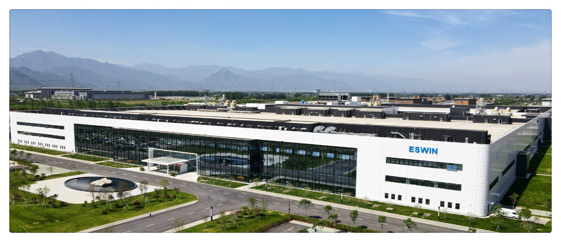
ESWIN selects advanced equipment and processes, in combination with the highest level of clean room design and production control, to manufacture super-flat, superior nanotopography 12-inch silicon wafers that are free of dislocations or intrinsic flaws. At present, ESWIN owns a silicon industry base in Xi'an, with a design production capacity of 500,000 pieces per month. Main products are monocrystalline silicon polished wafers and epitaxial wafers used in ICs. The applicable fields include logic IC, 3D NAND & Nor Flash, DRAM, CIS, and Display Driver IC, etc.

A silicon polished wafer is a wafer with mirror surfaces which is produced from a monocrystalline silicon ingot through processes including cutting, grinding, chemical-mechanical polishing and cleaning.
Processes: The high-purity poly-silicon materials are put into a quartz crucible, heated above 1400°C and then melt into silicon solution. Then the seed crystal is immersed in the solution, and then the pulling of a monocrystalline silicon ingot is completed after seeding, shoulder, body growth and tail steps. The finished monocrystalline silicon ingot is then cut into 300-400mm-long silicon blocks. Then the blocks are sliced into 1mm-thick slices by linear cutting,then the slices are polished and cleaned to be high quality polished wafers.
Application fields: 12-inch polished wafers are widely used in NAND flash ICs and DRAM memory ICs.
The epitaxial wafer is a silicon wafer with a monocrystalline film that is formed on the substrate of silicon polished wafer through epitaxial growth.
Processes: Chemical vapor deposition technologies are adopted to produce high-quality mono crystals that are epitaxially arranged on the polished wafer in an orderly manner.
Application fields: 12-inch epitaxial wafers are widely used in CPU/GPU and other logic ICs, power devices such as MOSFET/IGBT, and image sensors.